Skip to main content
Toggle navigation
Home
About-Us
About Headpcb
Why Headpcb
Quality Assurance
Capability
Mission
HR Concept
Social Responsibility
Privacy Policy
Products
Quick Turn Prototype
Seamless PCB Production
Rigid-PCB
Flex-PCB
Rigid-Flex-PCB
Aluminum-PCB
Special-PCB
SMD Stencil
Quality
Quality Control
RoHS Control
Design Rule Check
E-Test
AOI
X-RAY
CCD
Impedance Control
Equipment
PCB-Equipment
FPC-Equipment
Test-Equipment
News-Blog
Contac-Us
Home
>
>
Rigid-PCB
>
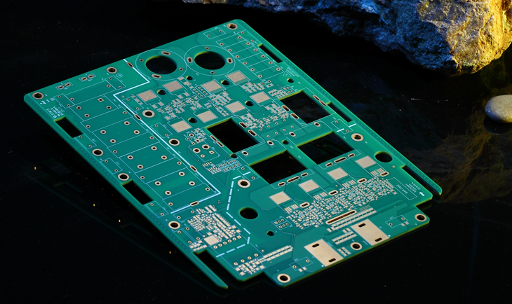
Copper Paste Filling PCB
Copper Paste Filling PCB
Project Description
|
Parameters
4 Layer
Thickness: 2.05+/-0.2 mm(High Tg)
Min Hole Size: 0.2 mm
Width/Space: 0.1mm/0.1 mm
Surface Treatment: ENIG
|
Craft
Copper Paste Filling
|
Application
Indstrial Control
Related Portfolio
VIEW LARGE
2 Layer Board
VIEW LARGE
4 Layer OSP+ENIG PCB
VIEW LARGE
6 layer heavy ENIG board
VIEW LARGE
Countersink PCB