PCB Board Manufacturing is printed circuit boards manufacturing . Headpcb is one of the PCB Board manufacturer in china , Have 18 years experience on PCB board manufacturing . PCB Capability 1 - 36 Layers .

At Headpcb team utilizes the latest in PCB technology and equipment to meet the demand for quality. Our dedication to providing quality PCB products and services have helped us earn the trust and respect of our customers.
We constantly work towards creating innovative solutions, and we spare no expense in acquiring the latest in PCB board manufacturing technologies and an experienced workforce. This places us in a strong position to provide top notch services, from PCB manufacturing to assembly ,testing and delivery.
PCB Board Manufacturing Steps
First :PCB Film Generation
Films for all of the copper and soldermask layers are made from photographically exposed mylar. We generate these films from your design files, creating an exact (1:1) film representation of your design. When Gerber files are submitted, each individual Gerber file represents one layer of the PCB Board .
Second :PCB Select Raw Material
Industry standard 1.6mm thick FR-4 laminate copper clad on two sides. Panels will be sized to accommodate many boards.

3rd :PCB Drill Holes
Through holes required for your PCB design are created from your submitted files, using NC drill machines and carbide drill bits.

4th : PCB Electroless Copper
In order for the through holes to electrically connect to different layers of the PCB, a thin layer of copper is chemically deposited into the through holes. This copper will later be thickened through electrolytic copper plating (step 6th).
5th :PCB Apply Photo-resist and Image
To transfer the PCB design from the electronic CAD data to the physical circuit board, we start by applying photosensitive photo-resist to the panel,covering the entire board area. Then the copper layer film image (step first ) is placed over the board, a high intensity UV light source exposes the uncovered portion of the photo-resist. Then we chemically develop the board (remove the unexposed photo-resist from the panel) creating the pads and traces.

6th : PCB Pattern Plate
This step is an electrochemical process which builds copper thickness into the holes and onto the surface of the PCB. Once the copper thickness is built up on the circuitry and in the holes, we plate and additional layer of tin to the exposed surface. This tin will protect the plated copper during the etching process (step 7th ) and be later removed.
7th:PCB Strip & PCB Etch
This process takes place in multiple steps. The first is to chemically remove (strip) the photo-resist from the panel. Then the newly exposed copper is chemically removed (etched) from the panel. The tin applied in step 6 protects the desired copper circuitry from being etched. At this point, the fundamental circuitry of the PCB is defined. Finally, the protective layer of tin is chemically removed (stripped) to expose the copper circuitry.
8th :PCB Soldermask
Next we coat the entire panel with a liquid soldermask layer. Using films and high intensity UV light (similar to step 5th) we expose the solderable areas of the PCB. The main function of the soldermask is to protect the majority of the copper circuitry from oxidation, damage and corrosion as well as maintain isolation of the circuits during assembly.

9th: PCB Legend (silkscreen)
Next we print the reference designators, logos, and other information contained in the electronic files onto the panel. This process is very similar to an inkjet printing process, but designed specifically for PCBs

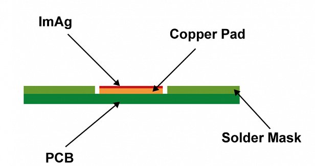
10th : PCB Surface Finish
The final surface finish is then applied to the panels. This surface finish (tin / lead solder or immersion silver,gold plating ) is used to protect the copper (solderable surfaces) from oxidation as well as act as a site for soldering of components to the PCB.

11th: PCB Fabrication
Finally , but not least, we route the perimeter of the PCB from the larger panel using NC equipment. The PCB board is now complete, and is quickly shipped to you.
This is single side PCB and double sided PCB board manufacturing process , Multi-layer PCB board manufacturing will be more complicate . need press lamination .
After 11 PCB manufacturing steps , We will do 100% Electronic E-test for your PCB board .
Headpcb is your premier source, with the most competitive pricing in the industry and a commitment to total customer satisfaction.