What is Aspect Ratio in PCB industry?Wednesday,May 25,2016
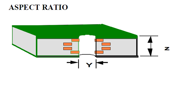
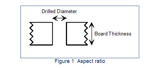
In PCB fabrication the aspect ratio is the thickness of a PCB divided by the diameter size of a drilled hole — see Figure 1 below. It's importance relates to the plating process — plating solutions must flow through the hole efficiently in order to achieve acceptable copper plating. Hole sizes that are small compared with the board thickness can result in unsatisfactory plating.
The larger the aspect ratio, the more difficult it is to achieve reliable plating.
Figure 1 above shows a graphical representation of how the aspect ratio is calculated; for example, a 0.7mm finished hole size in a 1.6mm PCB will give an aspect ratio of 1.6mm / 0.8mm therefore 2:1, regarded as a very safe ratio. (Note the drill diameter size used to calculate the ratio is 0.1mm larger than the finished hole size this is to allow for plating down the barrel of the hole. This value can vary between manufacturers.) All manufacturers should be able to achieve aspect ratios of up to 6:1; very small holes in thick boards (i.e. > 10:1 ratio) are possible, but usually at a cost.
In today's PCB industry, standard Aspect Ratio is 8:1, that is If board thickness is 1.6mm, hole size must be >=0.20mm If board thickness is 2.0mm, hole size must be >=0.25mm If board thickness is 3.0mm, hole size must be >=0.373mm ...
At Headpcb, we are able to reach to 10:1 Aspect Ratio, that is If board thickness is 1.6mm, hole size must be >=0.16mm If board thickness is 2.0mm, hole size must be >=0.20mm If board thickness is 3.0mm, hole size must be >=0.30mm ...
Recommend using 0.2mm vias or larger as a standard practice, this will help keep cost down, reliability up, and ease the pains of manufacturing.
|