An Introduction to HDI (High Density Interconnector) PCBMonday,May 08,2017
What are HDI PCBS?HDI PCBs are one of the fastest growing technologies in the field of PCB manufacturing. Anyone affiliated or interested in this industry is sure to come across this term every now and then. And if your company isn’t using them, you better start now. So the question lies, what are exactly HDI PCBS?  HDI PCBs (High Density Interconnector) are essentiallya type of circuit board which has a higher wiring density per unit area as opposed to conventional boards. HDI PCBs help to make room on your printed circuit board while increasing their efficiency, allow for high frequency transmission, decrease redundant radiation etc. Characteristics of HDI PCBs: HDI PCBs have finer spaces and lines; have minor bias and increases connection pad density. The board has an overall increase in density because of the miniaturization and arrays of the electric parts. An HDI PCB usually consists of blind and buried vias and often microvias that are 0.006 or less in diameter.The placement of the parts requires extra precision because of the miniature pads and the fine pitch of the circuit board.  Benefits of HDI PCBs: By the use of HDI technology, designers can place more components on both sides of the RAW PCB according to requirements. The placement of smaller components closer together is also possible. The overall result is faster transmission of signals and reduction in loss of signals and delays. 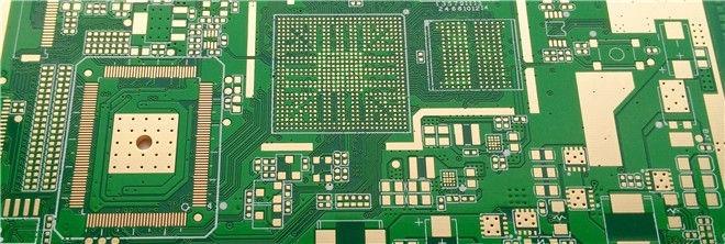 HDI PCBs are used to reduce the weight and dimension of products and to enhance efficiency of the device. HDI PCBs are taking advantage of the latest tech to amplify the functionality of PCBs in less area. You can find HDI PCBs in mobile phones, touch screen devices, laptops, computers, cameras, and even medical devices, and aircraft devices. The possibilities are endless. Applications of HDI PCBS: As mentioned before, the possibilities of the uses of HDI PCBs are endless. The common reason is increase in packaging density. They improve HDI PCB function by stabilizing power usage, reducing interference induction, improving signal integrity and also have faster routing capabilities. This is why you will find them in all kinds of industries.  One of the fields we mentioned is the medical field. Medical devices often require smaller size and high transmission rate which fortunately, is what HDI PCBs deliver. The perfect example is an electronic implant. It must be small enough to it into the human body but also must function with high-speed signal transmission. They are also used in monitoring devices, CT scanners etc. Conclusion: In 1992, the average cell phone weighed 220 to 250 grams and did not have the functionality present day mobiles offer. Today we have devices weighing 151 grams or even less with endless applications. This is all made possible with the help of HDI PCB technology. Similarly products will keep getting smaller with increased efficiency. This will help us to push technology to smaller and lighter requirements for our daily use. |