PCB SideplatingMonday,Aug 21,2017
PCB Sideplating1. The definition of Sideplating
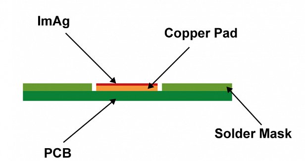
Sideplating is actually the metalization of the board edge in PCB filed. Edge plating、Border plated、plated contour、side metal, these words can be used too to describe same function. 2. Sideplating Process Drilling - Milling plated Slots - Cleaning - Copper sink 3. Pictures to show the finished board’s sideplating  4. Possible applications of sideplating: 4.1 Improvement of EMC performance by shielding the inner region of multilayer_s (eg for HF circuit boards 4.2 Cooling function with the edge as additional cooling surface, where an active heat dissipation can be used 4.3 Housing connection 4.4 Board-on-Board connection (see plated half-holes) 5. Design Parameters To guarantee the producibility of the sideplating, the metallized area must be defined using overlapping copper (copper surface, pads, or tracks) in the CAD layout. Minimum overlap:500mm. On the connected layer, min 300um of connected copper must be defined. On non-connected layers, the copper should have gap of min. 800um from the outer contour.  5. Usually , we recommend customers to make immersion gold or immersion silver for edgeplating. When design the solder mask layer, it should be solder mask opening in the file. Also you can show us some texts to show the detailed requirements.
|