High Frequency PCB Design TechniquesTuesday,Jan 16,2018
Author: David Jones
High frequency design is where you really need to consider the effects of parasitic inductance, capacitance and impedance of your PCB layout. If your signal is too fast, and your track is too long, then the track can take on the properties of a transmission line. If you don’t use proper transmission line techniques in these situations then you can start to get reflections and other signal integrity problems. A “critical length” track is one in which the propagation time of the signal starts to get close to the length of the track. On standard FR4 copper boards, a signal will travel roughly 6 inches every nano second. A rule of thumb states that you need to get really concerned when your track length approaches half of this figure. But in reality it can actually be much less than this. Remember that digital square wave signals have a harmonic content, so a 100MHz square wave can actually have signal components extending into the GHz region.
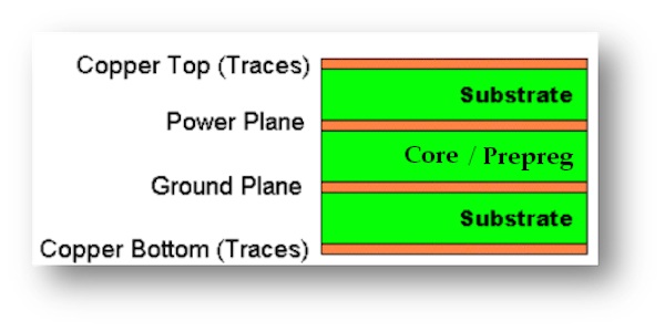
In high speed design, the ground plane is fundamental to preserving the integrity of your signals, and also reducing EMI emissions. It allows you to create “controlled impedance” traces, which match your electrical source and load. It also allows you to keep signals coupled “tight” to their return path (ground).
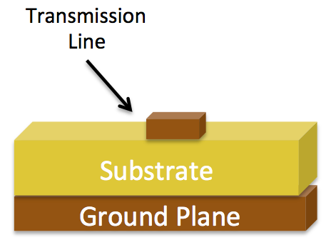
There are many ways to create controlled impedance “transmission” lines on a PCB. But the two most basic and popular ways are called Microstrip and Stripline. A Microstrip is simply a trace on the top layer, with a ground plane below. The calculation involved to find the characteristic impedance of a Microstrip is relatively complex. It is based on the width and thickness of the trace, the height above the ground plane, and the relative permittivity of the PCB material. This is why it is important to keep the ground plane as close as possible to (usually) the top layer.
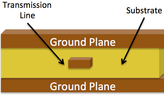
A Stripline is similar to the Microstrip, but it has an additional ground plane on top of the trace. So in this case, the trace would have to be on one of the inner layers. The advantage of stripline over microstrip is that most of the EMI radiation will be contained within the ground planes.
There are many free programs and spreadsheets available that will calculate all the variations of Microstrip and Stripline for you.
Some useful information and rules of thumb for high frequency design are: 1) Keep your high frequency signal tracks as short as possible. 2) Avoid running critical high frequency signal tracks over any cutout in your ground plane. This causes discontinuity in the signal return path, and can lead to EMI problems. Avoid cutouts in your ground plane wherever possible. A cutout is different to a split plane, which is fine, provided you keep your high frequency signal tracks over the relevant continuous plane. 3) Have one decoupling capacitor per power pin. 4) If possible, track the IC power pin to the bypass capacitor first, and then to the power plane. This will reduce switching noise on your power plane. For very high frequency designs, taking your power pin directly to the power plane provides lower inductance, which may be more beneficial than lower noise on your plane. 5) Be aware that vias will cause discontinuities in the characteristic impedance of a transmission line. 6) To minimize crosstalk between two traces above a ground plane, minimize the distance between the plane and trace, and maximize the distance between traces. The coefficient of coupling between two traces is given by 1/(1+(Distance between traces / height from plane)^2)) 7) Smaller diameter vias have lower parasitic inductance, and are thus preferred the higher in frequency you go. 8) Do not connect your main power input connector directly to your power planes, take it via your main filter capacitor(s).
|