Via-in-Pad PCBTuesday,Jul 10,2018
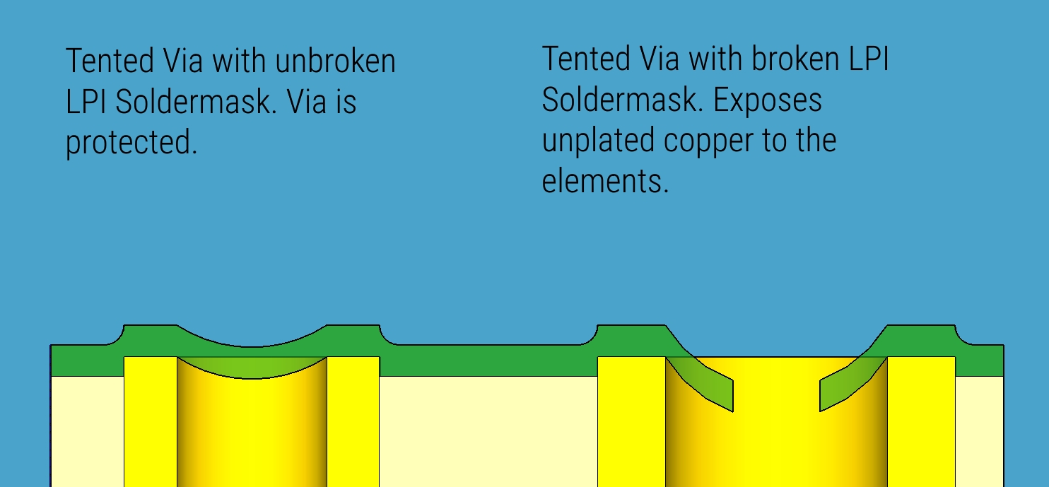
PCB Via-in-Pad When it comes to Vias, it’s known to us all that Vias can be divided into Through-hole Vias, Blind Vias and Buried Vias. They have different functions.
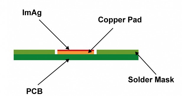
 With the development of the electronic products, Vias play a vital role in the interconnection between layers in a printed circuit board, The application of Via-in-Pad is widely in small-scale PCBs and BGA((ball grid arrays).As the necessary high-density BGA (Ball Grid Array) and SMD chip miniaturization, the use of Via-in-Pad technology has become increasingly significant.  Compared with bind hole and buried hole, Via-in-Pad technology has a lot of advantages:
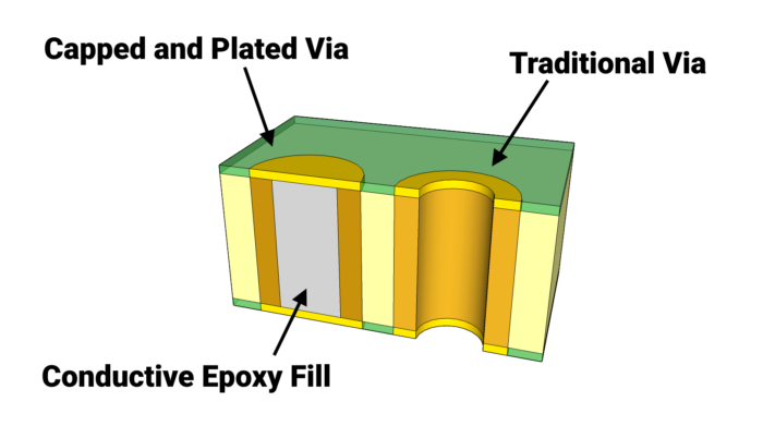
With the reliable Via filling/capping process, Via-in-Pad technology can be used to produce high-density PCB designs without the use of chemical enclosures, avoiding soldering errors.In addition, this can provide the BGA with additional conductor traces.
|