How important is Dielectric Constant to your PCB Design?Monday,Jul 25,2016
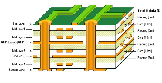
The board stack-up is probably the most essential piece for ensuring a successful PCB design. Modern high-speed boards require controlled-impedance traces, and whether you are using a simulation tool, a simple calculator, or the back of a napkin, you need to understand your manufacturing process to correlate your impedance calculations. This ensures that your trace widths and dielectric heights match what will actually be manufactured, and eliminates last-minute design changes.
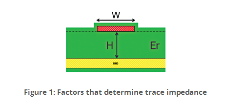
Impedance Determination Impedance is what drives the dielectric thicknesses and trace widths in the board. Figure 1 shows the three main factors in determining trace impedance: trace width (W), height above the reference plane (H), and dielectric constant (Er). Trace impedance goes up as H goes up, and impedance goes down as W and Er go up. Impedance numbers can be calculated by using formulas or calculator tools, but the most accurate data will be generated from a field solver. Signal integrity simulation tools such as HyperLynx from Mentor Graphics have built-in field solvers, and can be used to generate stackup geometry numbers for a given impedance.
When determining W and H, you can typically begin with a W of 4 mils, as that usually is the minimum manufacturable trace width on ½-oz. copper without incurring extra cost. This is usually the starting point for determining layer height. Since the highest impedance is obtained by using the minimum trace width and maximum dielectric height, the dielectric height is set by the highest impedance needed for the layer using a 4-mil trace width. For instance, if the maximum impedance needed on a given layer is 60 ohms, the dielectric height for that layer would be set to about 5 mils, since a 4-mil trace with a 5-mil dielectric height will be 60 ohms (given an Er of about 3.6).
In doing these calculations, it is imperative to use the correct value for dielectric constant, as that is where most discrepancies between your calculations and the board fabricator’s calculations can differ. Most important is the fact that Er can vary with different dielectric thicknesses due to variations in glass and resin content. Typical values for FR4 material range between 3.5 and 4.5, so it is important to talk to your board manufacturer to get the right values. More often than not, smaller dielectric thicknesses are used in a design, and these typically have lower dielectric constants. For FR4, most people just use an Er of 4. This means that their trace widths and dielectric heights get designed for an impedance lower than what will actually be manufactured, since the dielectric constant is most likely lower (and, if you recall from above, as Er goes down, impedance goes up).
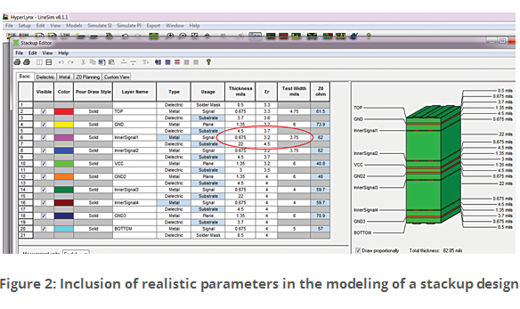
Board Material Variation Another aspect of real PCB fabrication that can cause you to shoot for too low of an impedance target is failure to take into account the variation of glass/resin content around the traces. When multiple PCB layers are pressed together, the resin tends to flow into the spaces around the traces, creating a resin-rich area around the traces that will have a lower dielectric constant. As such, it is important to model that lower Er when modeling your board stack-up. Figure 2 shows an example of this in the HyperLynx Stack-up Editor, where an Er of 3.2 is assigned to the trace layer in the stack-up to mimic the results of actual board fabrication.
Use of incorrect dielectric constant values can also throw off timing calculations in simulation. You can notice a difference of up to about 100ps for a 10-in. trace, which can be quite detrimental to design margins.
It is also important to realize that when traces are manufactured, the etching process can leave them in more of a trapezoidal shape than a rectangle. For a ½-oz. trace, this can lead to a difference in trace width from top to bottom of about 0.5 mils. This effect should be included when modeling the traces, and is easily approximated by assigning the mean width of the actual trace to the trace width. For a ½-oz. trace, that would mean subtracting 0.25 mils from the target trace width. This is also included in Figure 2.
Summing Up As you can see, most of the causes for discrepancy between simulated and actual impedance result in too low of an impedance in the simulation. In fact, in Figure 2 above, you may notice that the lower half of the stackup (a mirror image of the top) is modeled without taking into account actual dielectric constant, the resin-rich area around the traces, or the proper trace width. You will notice discrepancies in impedance for equivalent layers and traces. In some stackups, this difference can be up to about 5 ohms. This becomes problematic because the fab house will have to widen the trace or increase the dielectric thickness to compensate for the miscalculation, which can lead to possible manufacturing issues. For instance, if a trace is spaced the minimum clearance from an object like a pin or via and then becomes widened, it could become too close to that object. Similarly, enlarged dielectric layers may cause the total board thickness to fall out of spec. This is why it is best to work with your board manufacturer to get accurate data about your board stackup, to make sure that your design specs are within reason and can be maintained, and that you don’t run into problems later in the design cycle.
|